SAW Grade LiNbO3 Crystal & Wafer
SAW Grade LiNbO3 Crystal & Wafer
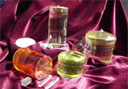
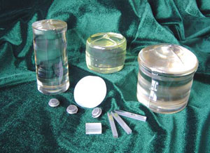
Lithium niobate (LN) crystals have excellent piezoelectric, electro-optic, acousto-optic and nonlinear properties. In the civil field has a wide range of uses, with the development of photoelectric technology, LN crystal is still a good piezoelectric crystal, can be used to make low-frequency SAW filter, high-power high temperature resistant ultrasonic transducer and so on.
| Item | Model | Specification |
| 1 | Lithium niobate substrate and crystal | Φ2″Y-cut,Z-cut,X-cut |
| 2 | Lithium niobate substrate and crystal | Φ2″64°Y-X |
| 3 | Lithium niobate substrate and crystal | Φ2″128°Y-X |
| 4 | Lithium niobate substrate and crystal | Φ3″Y-cut, Z-cut |
| 5 | Lithium niobate substrate and crystal | Φ3″64°Y-X |
| 6 | Lithium niobate substrate and crystal | Φ3″128°Y-X |
| 7 | Lithium niobate substrate and crystal | Φ4″Y-cut Z-cut |
| 8 | Lithium niobate substrate and crystal | Φ4″64°Y-X |
| 9 | Lithium niobate substrate and crystal | Φ4″128°Y-X |
Basic Properties
| Crystal Structure | Trigonal, point group3m |
| Lattice Parameters | a=5.148, c=13.863 |
| Density | 4.64g/cm3 |
| Melting Point | 1250℃ |
| Curie Point | 1142±2℃ |
| Mohs Hardness | 5 |
| Dielectric Constant | ε11/ε0=85; ε33/ε0=29.5 |
| Thermal Conductivity | 38W/m/℃ at25℃ |
| Thermal Expansion Coefficient | a1=a2=2*10-6/℃, a3=2.2*10-6/℃ at25℃ |
| Piezoelectric Strain Constant | d22=2.04*10-11C/N,d33=0.6*10-11C/N, d15=7X10-11C/N,d31=-0.1X10-11C/N |
| Elastic Stiffness Constant | C11E=2.04*1011N/m2,C33E=2.46*1011N/m2, |
SAW Grade LiNbO3Wafer
| Orientation | 64°rot.Y-cut ± 0.2° | 127.86°rot.Y-cut ± 0.2° | Y-cut ± 0.2° |
| Diameter | 76.2mm±0.3mm 100.0mm±0.3mm | 76.2mm±0.3mm 100.0mm±0.3mm | 76.2mm±0.3mm 100.0mm±0.3mm |
| Orientation Flat (OF) | 22mm±2mm 22mm±2mm Perpendicular to X ± 0.2° | 22mm±2mm 22mm±2mm Perpendicular to X ± 0.2° | 22mm±2mm 22mm±2mm Perpendicular to X ± 0.2° |
| Second Refer. Flat (RF) | 10mm±3mm Cw180° ± 0.5° from OF | 10mm±3mm Cw225° ± 0.5° from OF | 10mm±3mm Cw270° ± 0.5° from OF |
| Thickness | 500um ± 20um 350um ± 20um | 500um ± 20um 350um ± 20um | 500um ± 20um 350um ± 20um |
| Propagating surface | “+” side Ra ≤ 8 | “+” side Ra ≤ 8 | “+” side Ra ≤ 8 |
| Wafer backside | GC#1000lapped & etched 0.2um≤Ra≤0.7um | GC#1000lapped & etched 0.2um≤Ra≤0.7um | GC#1000lapped & etched 0.2um≤Ra≤0.7um |
| TTV | ≤ 10um | ||
| LTV | ≤ 2.0um within an area of5×5mm2 | ||
| PLTV | ≥ 95% (3mmfrom edge excluded) | ||
| BOW | -25um ≤ Bow ≤ +25um | ||
| Curie Temperature | 1142℃±3℃(DTA method) | ||
| Edge Beveling | Edge rounding | ||
附件下载: